The ROM Board Project
Why and how
There are mainly three reasons why a substitute for the built-in ROM set might be useful:
- The built-in ROM set is defective and has to be replaced in order to get the system working.
- The built-in ROM set has an older revision and shall be upgraded to a version with more functionality, less bugs and a broader support for peripheral devices.
- There are errors during system start-up which prevent the system from booting, so boot-up diagnostics are required but an HP Test ROM is not available.
Replacing the 9845 ROMs, independent whether system ROMs for PPU or LPU or option ROMs are affected, is not an easy task. Replacing option ROMs is still somewhat more demanding, so we are looking first at the easier part, the system ROMs for the PPU and the LPU.
Before a solution for system ROM replacement is introduced, here are some basics about the ROMs in the 9845.
The 9845 ROM Philosophy
The 9845 has two independent processing units, the Language Processing Unit (LPU) and the Periperal Processing Unit (PPU). The whole address space is accessible by both processors (even in parallel) and divided into memory blocks of size 32k words or 64k bytes. Those memory blocks can be implemented either as RAM or as ROM space.
Technically, there is no requirement that specfic blocks have to be ROM and others have to be RAM, however there is an implementation rule which says: all even blocks are RAM (including block 0), and all odd blocks are ROM, with the exception of block one, which is the single RAM block which is primarily dedicated for use by the PPU. Consequently, all even memory blocks are reserved as LPU RAM, block 1 is the PPU RAM block, and all odd blocks starting at block number 3 are ROM blocks.
Those ROM blocks now are organized in the following way (all block numbers in decimal):
- Block 3 holds the LPU system ROMs
- Block 5 holds the PPU system ROMs
- Block 7, 11, 15, 19, 23 etc. are reserved for LPU option ROMs
- Block 9, 13, 17, 21, 25 etc. are reserved for PPU option ROMs
- Block 37 is the 'test ROM block', which after power-on is checked first for executable code, before execution is being directed to block 5
One of the advantages of the 9845 was that it didn't need a boot medium for operation. This results from the fact, that the whole operating system, including the development and runtime environment for 9845 BASIC, was completely built into firmware (i.e. ROMs). After some seconds of start-up diagnostics the system is literally "ready for use".
Today, this makes the system more sensitive to ROM failures. And this is a serious problem, since the original HP ROMs are real 'time bombs', as many of them fail due to aging. So preserving the original ROM content is one of the more important procedures, and there are two special section for this (look at the Dumping ROMs Tutorial and the ROM Dumping Project).
The System ROM Chips
Unfortunately, HP decided to use specially designed ROMs for their 9845 systems. The pinout differs from most 'standard' ROMs, and even worse, some of the address multiplexing logic is implemented into the ROMs, presumably to save space on the PCBs. This makes it a little bit harder to perform the standard exchange procedure in terms of just replacing the the ROMs by EPROMs with equivalent size and capacity.
The good news is that it is possible anyway. The original system ROM chips have a pinout which is identical the the pinout of the 2364 ROM chip (which is used in the common Commodore C64 home computers), and differs only in some pins from that of e.g. a 28C64 EEPROM, so an adaptor can be easily built. The built-in additional logic is not too complex, it just works as latches for the address as long as there is data and not address information on the shared address/data memory bus. This behavior can be implemented for a normal EEPROM by just adding two 74LS373 latches.
The ROM Board
Each system ROM set consists of eight ROM chips. Since the used chips have an 8kx8 organization, two chips are combined as lower and higher byte of an 8k word address space with 16-bit wide words. Four times one pair makes up eight chips or 32 kWords.
In principle, each defective ROM could be replaced by a small PCB holding one 28C64 EEPROM and two 74LS373 chips. But because the chance is good more than one system ROM will fail, it is probably the better way just to replace all system ROMs at once, e.g. by two 28C256 EEPROMS, which can provide the whole firmware for one single processor in just two chips (we cannot place the whole firmware into one single 512 kBit EEPROM, since we need 16 data lines for a 16 bit wide data bus). Of course we still need the latches, but still only two of those chips (2 x 8 bit latches).
For a full firmware replacement some additional problems must be solved. One challenge is, that the system boards are packed pretty close in the board cages, and there is not too much space between the RAM/ROM board and the neighbour board. In addition, the addressing signals for address lines 13 and 14 have to be mapped to the chip selection signals. And the EEPROM must know when there is a valid address on the shared address/data bus. So we need to guide a couple of extra signals to the replacement.
I made a basic design with two 28C256 EEPROMs, two 74LS373 8-bit latches, plus one 74LS32 OR-gate and one 74LS05 inverter, and prooved the design with a simple wire wrapped prototype. The prototype is still connected to the RAM/ROM board via ribbon cables, since the board doesn't fit between the RAM/ROM board and its neighbour (for the time beeing, it is placed into the printer's paper roll tray).
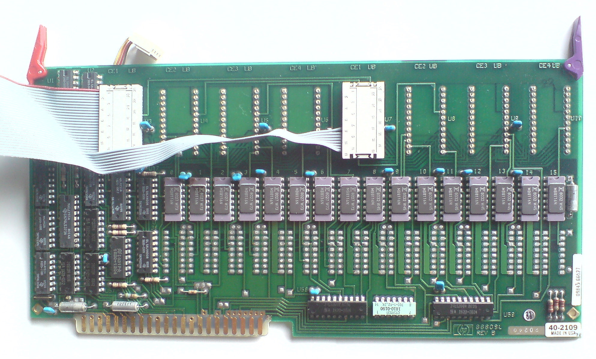
09845-66528 RAM/ROM Board with Ribbon Cable Connectors
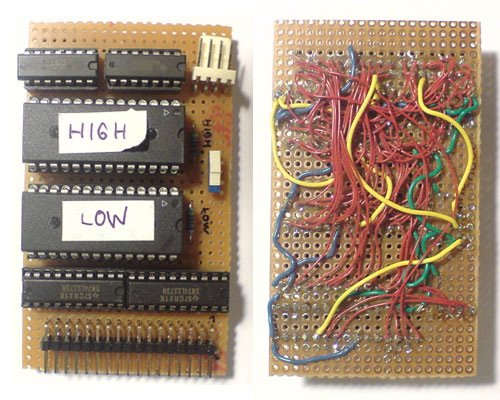
ROM Board Prototype (wire wrapped)
Most of the needed signals are provided by two of the ROM sockets. Four additional signals have to be derived from some soldering points from the back of the RAM/ROM PCB.
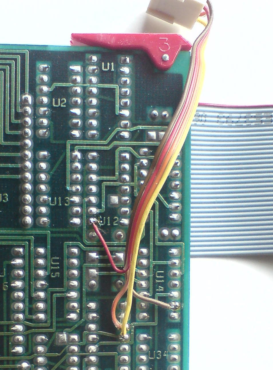
Soldering Points on 09845-66528 RAM/ROM Board (before and after soldering)
You can use your favorite EPROM programmer for transferring the firmware to the 28C256 EEPROMs, a willem programmer will do it. I've included a couple of firmware images in the download section below. Note that different 9845 versions need different ROM images. I've combined the latest available firmware revisions into each ROM image, and if you are using flash memory, you also can use the combined image set which provides the six most important images in one set. Get the ROM images from the downloads section below. Feel free to compose your own packages (see also the ROM Dumping project for all available firmware dumps).
Once the two EEPROMs are programmed, and all system ROMs from the 9845 RAM/ROM assembly are removed, and the replacement PCB is connected to the two ROM sockets and the four soldering points on the RAM/ROM assembly, this replacement works perfectly nice. There is no difference for the 9845, it just boots up as it is used to do. The replacement works both for the LPU and the PPU, since the PCBs are basically the same (they just differ in the number of DRAM chips installed and a jumper which identifies them as LPU or PPU RAM/ROM assembly and which selects the address space the boards are mapped to).
It is not that hard to build a version which fits as daughter board onto the 9845 RAM/ROM assembly. The component side of the daugther board should be oriented towards the 9845 RAM/ROM assembly, so the placement of the components depends on where there is some space on the 9845 RAM/ROM assembly (e.g. above the now empty LPU/PPU ROM sockets).
Important Note:
Since distance between the 9845 RAM/ROM assembly and the LPU assembly is limited (this is especially true for the bit slice LPU assembly), the solder side of the daughter board must be isolated properly towards to LPU assembly in order not to produce short circuits.
I've included a sample Eagle schematic plus two-layer board layout for use with two 29F0x0 flash memory chips.
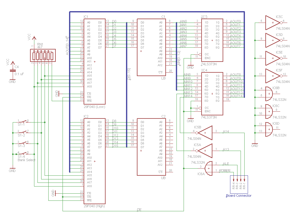
ROM Board Schematics (Eagle, click to enlarge)
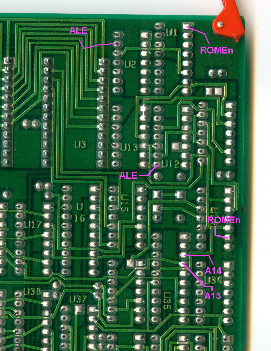
In the above schematics, note that the Low and High 9845 ROMs represent dual in-line pin arrays, which are plugged into the ROM sockets at position CE1/LB (U3) and CE1/UB (U7) on the 09845-66528 RAM/ROM assembly. The four extra lines soldered to the back of the 09845-66528 RAM/ROM assembly will be connected to the "Board Connector". The pins at the connector are mapped as follows in the above diagram:
RR-1 - A14
RR-2 - A13
RR-3 - ALE
RR-4 - ROMEn
Here are the components you need for the ROM board:
Qty. Components
2 29F0x0 flash ROMs (any 29F010, 29F020 or 29F040 would do and even 29C0x0 should work)
2 PLCC32 sockets (through-hole version, not SMD)
2 74LS373N octal transparent latches with three-state outputs
1 74LS04N hex inverter
1 74LS32N quad 2-input OR gate
1 7-pin 4.7 kOhms resistor network
1 .1uF ceramic capacitor for buffering the flash ROMs (optional but good habit)
1 4-switch DIP
1 4-contact molex connectors male + female for the "Board Connector"
The eagle data can be downloaded in the download section below. So you can home-brew the board as I did, or you can go to the next electronics shop and let them build the PCB for you from the Eagle and/or CAM data (please keep in mind that the provided layout is just a sample implementation).
Rik Bos occasionally produces some quantities of the ROM board and nicely offers them at cost price. If you're completely unhandy with soldering, he even may offer you the board built & tested for some nominal fee. Just use the contact feature and I'll forward your request.
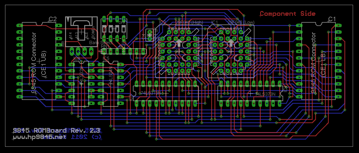
ROM Board PCB (current draft, click to enlarge)
The above PCB layout sample is designed as a two-layer daughter board for the 09845-66528 RAM/ROM assembly. The two 9845 ROMs represent the pin arrays which connect directly to the ROM sockets at the positions CE1/LB (U3) and CE1/UB (U7) on the 09845-66528 assembly. The component side of the PCB is oriented towards the 09845-66528 assembly. The DIP switch selects the appropriate firmware bank (up to four banks supported with using a 29F010 flash memory PLCC, or up to 16 banks with a 29F040).

ROM Board PCB
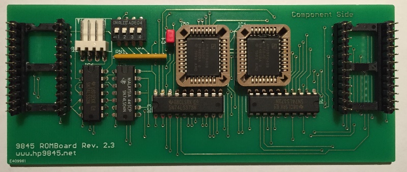
ROM Board PCB (Populated)
ROM Board Mounted on 9845 RAM/ROM Assembly (note transparent isolation sheet)
See How the ROM Board Fits (With Some Bending) Even With the Bit Slice LPU
Installed ROM Board (pretty tight, but it works)
Anyone who likes to make suggestions how the board layout can be optimized or who likes to develop an own solution, e.g. for a replacement of the whole RAM/ROM assembly including RAM (using an SRAM instead of the DRAMs would simplify the design) and address logic, should feel highly encouraged to do so.
A special case will be to build substitutions for the Option ROMs. There is a sample solution with the Mass Storage ROM from Structured Software Solutions, which is based on a special PCB design with two 2764 EPROMs, two 74LS373 and a PROM as address decoder, which fits completely into the size of an option ROM module. A schematic was reverse-engineered by Tony Duell as part of his 9845 schematics project. Maybe I'll publish an Eagle version as well in the future.
The probably most interesting application for an option ROM replacement would is to clone HP's rare original Test ROM, since it allows you to perform a couple of boot time diagnostics, even with defect system ROMs. Another great thing would be to develop a basic system monitor and place it into an option ROM, especially if it would allow to bootstrap via one of the peripheral interfaces.
For that reason, the full ROM image set (see download below) also includes a modified version of the original Test ROM, which allows
- booting with a minimum amount of RAM
- performing diagnostics of the HP9845 core system
- booting into a command line shell for inspection and diagnostics
- booting into an external operating system
- using remote keyboard and screen for input/output via GPIB connection (remote terminal)
Also see this page for more information on the Test ROM.
Downloads
Click here for downloading the firmware images and/or ROM board Eagle data:
| LPU 28C256 EEPROM images for systems equipped with a standard (hybrid) processor: | 9845-LPU-Standard-Processor.zip |
| LPU 28C256 EEPROM images for systems equipped with a fast (bit-slice) processor: | 9845-LPU-Fast-Processor.zip |
| PPU 28C256 EEPROM images for systems equipped with a standard (98750A) monochrome CRT display*: | 9845-PPU-Standard-Graphics.zip |
| PPU 28C256 EEPROM images for systems equipped with an enhanced monochrome (98780A) or color (98770A) CRT display*: | 9845-PPU-Enhanced-or-Color-Graphics.zip |
| Combined image set for 29F020 or 29F040 flash chips, bank selectable, includes all of the above images plus German keyboard support & 9845 Test ROM | 9845-ROMBoard-Imageset.zip |
| ROM board prototype schematics & PCB layout (Eagle & CAM data): | ROMBoard-Eagle-Data-20.zip |
| ROM board current (optimized) schematics & PCB layout (Eagle & CAM data): | ROMBoard-Eagle-Data-23.zip |
*PPU images include support for 09845-66590 512K RAM expansion boards.
Here are sample system firmware disassemblies for several 9845 configurations (see also the 9845 Assembler Project):
| System firmware disassemblies with cross reference, hexdump and string analysis for 4 selected system configurations (including firmware object code): | System-ROM-listings.zip |