The Processors
All 9845 were controlled by two processors working in parallel. One processor, the peripheral processing unit or PPU was responsible for all the I/O processing, like serving keyboard interrupts, writing data to the CRT display, or handling other peripheral I/O. The logical processing unit or LPU did execute all user programs, including BASIC programs and binary software modules.
For most systems, both processors were identical. The processor design went back on a very early minicomputer design, that of HP's first computer ever, the 2116A, which was transferred into a microprocessor design. So, much of the existing know-how and development environment of the 211x series could be recycled for the new processors. In fact, those processors were the first 16-bit microprocessors ever (as well as the 2116A had been one of the first 16-bit minicomputers before). Later HP introduced a modified high-performance version of the LPU, which was built on a custom bit-slice processor design, but still physically and electronically compatible to the original processors - the "hybrid processors".
The Hybrid Processors
The EMC was a quite powerful floating point processor. Unlike contemporary processors, but in the tradition of HP's calculators, all floating point numbers were represented by BCD mantissa and binary exponent, not in complete binary representation. The internal calculation range was -10511...-10-511,0,10-511...10511. Note that the BASIC interpreter cuts the exponent to a range from -99 to +99.
The 9845 series were not the first systems which used this hybrid processor. Almost the same type was already in use with the common 9825 series, as well as in some measuring equipment like the HP3585A spectrum analyzer (1978). The main change for the 9845 system with respect to the 9825 system was that the most significant address bit (the 16th bit) was no longer used for multi-level indirection addressing, but the address space was extended to 64 KWords (full 16 bit address space).
Later the address space of the hybrid processor was even more extended by a fourth NMOS chip, the address extension chip (AEC), which expanded the address space to (in principle) 65,536 memory blocks of 32 KWords each (= 4 Gigabytes!!!), and provided a very flexible kind of bank switching scheme. For the 9845 actually only 6 of the 16 possible AEC lines were utilized outside the processor, so the effective 9845 address space was in total limited to 64 memory blocks.
Dyke Shaffer was a late addition to the development of the HP9825/35/45 series and was responsible for the substrate design changes that extended the BPC/EMC/IOC hybrid to include the AEC device. After first writing a Fortran program on an HP2115 to analyze NMOS II artwork for design rule violations, to extract node capacitance and produce spice netlist, he joined the HP9835 development team to assist in the implementation of the new BPC hybrid substrate.
This turned out to be a significant effort due to the fact that the HP9825's 82 pin hybrid as it was initially released to production had a significant noise problem that had to be solved to produce the HP9835's 107 pin version. The new BPC hybrid was first developed for the HP9835 and later incorporated into the HP9845 as a cost reduction.
The elimination of the root cause of the noise first required that an awareness of its existence be documented and then addressed by careful choice of pin assignments in the 107 pin version to accommodate the additional AEC address signals. Eventually, a new version of the 82 pin substrate was designed and retrofitted back into the HP9825.
In addition to the substrate design and noise investigation, Dyke also built the second generation production test system that accommodated all of the BPC hybrid versions. This required a rack full of test equipment, a test program and custom binary commands be implemented for the HP9825 to control a pair of electronic tools (ET10161 and ET10162) that allowed the BPC hybrids to be automatically tested. Provision in the industrial design of the test head was made for trouble shooting the various BPC hybrids during assembly.
There were 14 boards that were designed and built by Dyke that were first implemented in
wire wrap form which was used in production for several years during which time the pc board layout and industrial were completed to release the two electronic tools and their enclosures.
There were two hybrid test systems eventually built to serve as production test for the last
10 years of production until the BPC hybrid was retired.
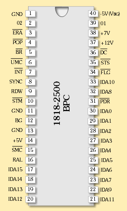
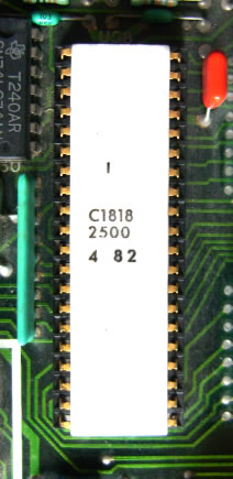
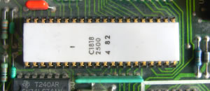 Also there was a BPC-only version of the processor (p/n 1818-2500) which had its first application in the HP 9871A daisy-wheel impact printer (introduced in 1975) and later in the 9872 series plotters (1977), in the 9874A digitizers (1978) and the 9875A dual tape cartridge drive (1978).
This BPC-only processor was provided in a 40-pin DIL package and was used with external bidirectional buffers (p/n 1820-1584) and 16-bit RAM/ROM.
Here is an overview of the known hybrid processor variants:
| Part No. | Used in | # Pins | Description |
| 09825-67907 | 9825 series, 3585A spectrum analyzer | 82 | Original version of the hybrid processor, still with multi-level indirection support |
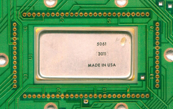
| 5061-3010 | 9845A (LPU) | 82 | Revised version of the hybrid processor, with extended address space, sacrifying the seldom-used multi-level indirection feature |
| 5061-3011 | 9845A (PPU), 4955A protocol analyzer, HP64000 development system | 82 | Special variant of the 5061-3010 hybrid processor without Extended Math Chip (EMC) |
| 5061-3043 | HP 250 | 82 | Variant of 5061-3010 hybrid processor used in the HP 250 system (same pinout as 5061-3010) |
| 5061-4204 | 8566A/8568A spectrum analyzer | 82 | Variant of 5061-3010 hybrid processor used in the HP 8566A/8568A spectrum analyzers (probably same pinout as 09825-67907, but with heat sink fins lengthwise instead of crosswise) |
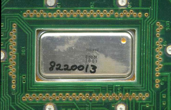
| 5061-3001 | 9845B/C, 9835A/B | 107 | Final design for the 9835A/B, 9845B and 9845C series, including the Address Extension Chip (AEC), was used both for the LPU and the PPU |
| 1818-2500 | Several peripheral devices | 40 | Stripped-down BPC-only version in a DIL ceramic package |
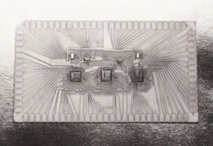
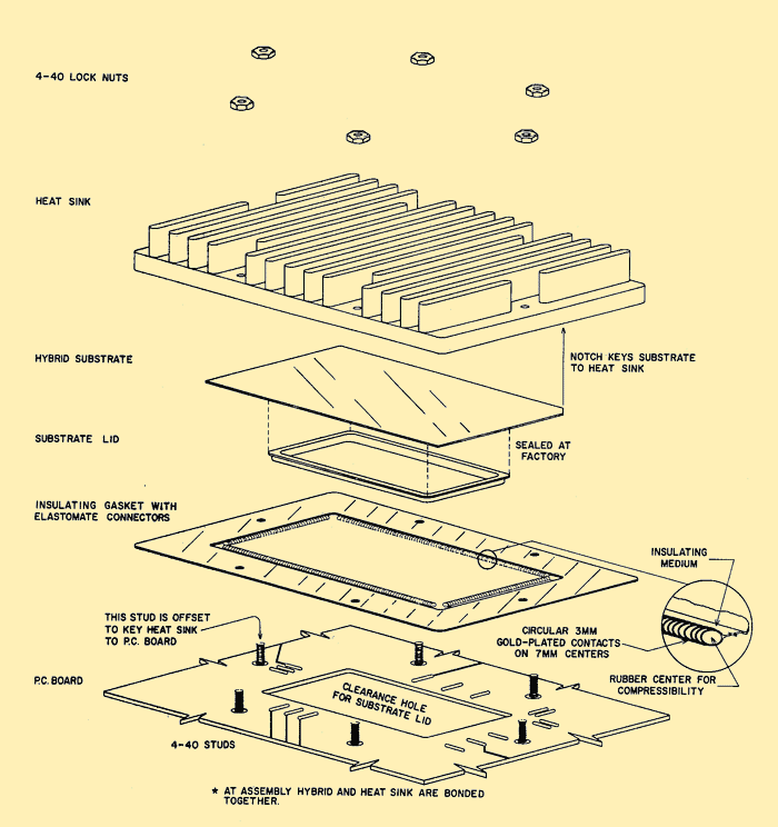
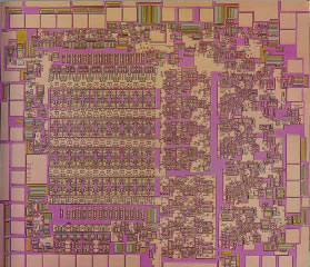
At design time in 1972/73 the whole functionality did not fit on one single chip (with roughly 18,000 transistors for the processor logic the die would have been too large for the production processes of the time), so the features were split into three single chips mentioned above (each of the three chips with a complexity comparable to the Intel 8080). BPC, IOC, EMC and BIBs were placed on a ceramic substrate with single layer gold connection paths.
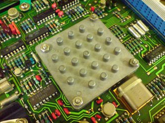
In contrast to other microprocessor packages, the hybrid processor was not connected to the circuit board via pin arrays, but through gold-wired elastomer cylinders which connected the pads of the board with those of the package with perfect alignment and well-calculated pressure. Not too different from todays multi-core processors, and quite similar to ceramic leadless chip carriers technology (CLCC) - but a wonder that this connection still works well even after almost 30 years.
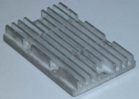
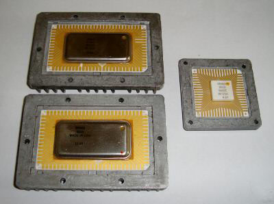
Due to direction of air flow, most hybrid processors are equipped with heat sinks with crosswise fins (see photograph above), except the 8566A/8568A spectrum analyzers, which used a heat sink with lengthwise fins.
Hybrid Processor Package with Heat Sink
One of the weird things was that both processors initialized after power-up with the same firmware code, until each processor tested for the status of a certain signal line in order to know whether it is the PPU or the LPU. Even more curious, at the 9845B and 9845C the signal was derived from the CRT vertical retrace, so that it required several tries to be sure that the signal is present.
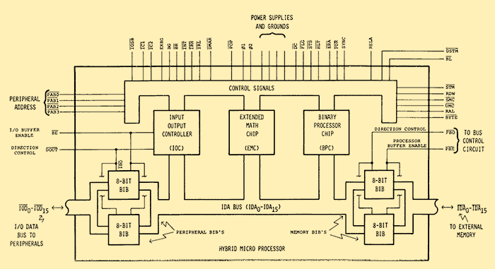
Processor Block Diagram (9845A LPU)
The processor architecture was straight-forward and didn't differ much from that of other microprogrammed processors of that time. Each chip consisted of a set of registers, the microcommand logic and one or two ROMs containing the microprograms. The registers were used for execution control, memory reference or temporary storage. Two accumulators, the A and the B registers, were used as general purpose registers. Two pairs of registers, the C/Cb and D/Db registers were used as stack pointers, three registers, the Dmac, Dmama and Dmapa controlled the DMA functions. The P register was used as program counter, the peripheral address register Pa was used to select the proper I/O channel. The return stack pointer R established a multi-level subroutine scheme. The Shift-extend register Se was used for external registers, a set of four registers were used for communicating with I/O devices. And, finally, a set of four words building the internal BCD arithmetic register AR2. A second BCD arithmetic register AR1 is stored in external R/W memory at address octal 177770-177773.
There are less documented registers like the interrupt vector register IV at address octal 10 or the working register W at address octal 12. All registers (except the AR1 register) were mapped into the memory address space at the addresses octal 0-37, so this part of memory is NOT available for ROM or R/W memory access (so to say, the first 32 words in each ROM or RAM address space are wasted).
Here is a complete overview of the hybrid processor registers:
| Address (octal) |
Mnemonic | Chip | Purpose |
| 0 | A | BPC | General purpose arithmetic accumulator |
| 1 | B | BPC | General purpose arithmetic accumulator |
| 2 | P | BPC | Program counter |
| 3 | R | BPC | Return stack pointer |
| 4 | R4 | IOC | I/O register |
| 5 | R5 | IOC | I/O register |
| 6 | R6 | IOC | I/O register |
| 7 | R7 | IOC | I/O register |
| 10 | IV | IOC | Interrupt vector (reserved) |
| 11 | Pa[0..3] | IOC | Peripheral address register |
| 12 | W | IOC | Working register (reserved) |
| 13 | Dmapa[0..3], Cb[15], Db[14] | IOC | DMA peripheral address register, block bits for byte pointer in C & D (read-only) |
| 14 | Dmama | IOC | DMA memory address register |
| 15 | Dmac | IOC | DMA count register |
| 16 | C | IOC | Stack pointer |
| 17 | D | IOC | Stack pointer |
| 20 | AR2 (0) | EMC | BCD arithmentic accumulator (LSW) |
| 21 | AR2 (1) | EMC | BCD arithmentic accumulator |
| 22 | AR2 (2) | EMC | BCD arithmentic accumulator |
| 23 | AR2 (3) | EMC | BCD arithmentic accumulator (MSW) |
| 24 | Se[0..3] | EMC | Shift-extend register |
| 25 | -reserved- | EMC | Internal BCD arithmetic register (reserved) |
| 26 | -reserved- | EMC | Internal BCD arithmetic register (reserved) |
| 27 | -reserved- | EMC | Internal BCD arithmetic register (reserved) |
| 30 | -reserved- | n/a | reserved |
| 31 | -reserved- | n/a | reserved |
| 32 | R32 | AEC/MAE | Indirect memory access for upper half of address space |
| 33 | R33 | AEC/MAE | Instruction fetch for lower half of address space |
| 34 | R34 | AEC/MAE | Instruction fetch for upper half of address space |
| 35 | R35 | AEC/MAE | Indirect memory access for lower half of address space |
| 36 | R36 | AEC/MAE | Base page addressing |
| 37 | R37 | AEC/MAE | Direct memory access |
In addition to the registers which were externally accessible, the processor included internal registers for the flags (decimal carry, extend and overflow).
The 9845A had both PPU and LPU on one assembly, the 9845B and 9845C used seperate boards in order to provide each processor with its own memory address extension and memory controller.
The Bit-slice Processor
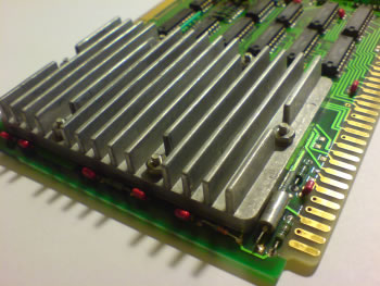
Probably inspired by the design of the 9845C where an AMD2900 bit-slice processor is used in the 98770A CRT display for the vector generator, there was a replacement developed by HP for the LPU hybrid processor which used the same AMD2900 approach as in the 98770A. The basic idea was to implement the most demanding BASIC interpreter routines into microcode in order to accelerate the system by an average factor of 5 to 7 (not a completely new idea, Wang Laboratories already had a similar approach eight years before with their 2200 minicomputers). The new 9845 systems which were equipped with the bit-slice LPU were called 9845 option 200. The bit-slice or fast LPU option was available both for the 9845B and the 9845C.
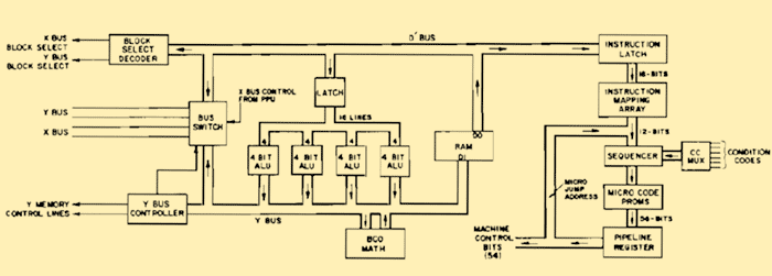
Bit-slice Processor Block Diagram
The idea behind the AMD2900 was simple but impressive. The 2900 family consists of a number of building blocks which can be used to set up a microprogrammed controller which is sufficient flexible to emulate existing machines. The whole bit-slice processor can be separated in two parts, the processing and the control section.
The processing section is built by an array of several 2901 four-bit bipolar microprocessor "slices", each including a 4-bit-wide 16 word RAM, high-speed ALU, shifting, decoding and multiplexing circuitry.The control section is implemented by a 2910 microprogram controller, which gets its instructions from a PROM holding 56-bit wide very long instruction words (VLIW).
For the 9845 model 200 bit-slice processor, a 2910 microprogram controller was combined with an array of four 2901 microprocessor slices, a 2 KWord 56-bit-wide control instructions PROM, and a BCD math unit built with discrete logic components, resulting in a 16-bit wide processing unit.
The bit-slice processor used the fast bipolar 2901 ALUs plus the discrete math logic to emulate the hybrid LPU and at the same time implement time critical routines from the BASIC interpreter in microprograms. This is the reason why on the one side BASIC programs are accelerated up to a factor of seven, on the other side assembler programs and binary routines do not profit from acceleration (in fact, assembler programs have been reported to run slightly slower than on a real hybrid LPU).
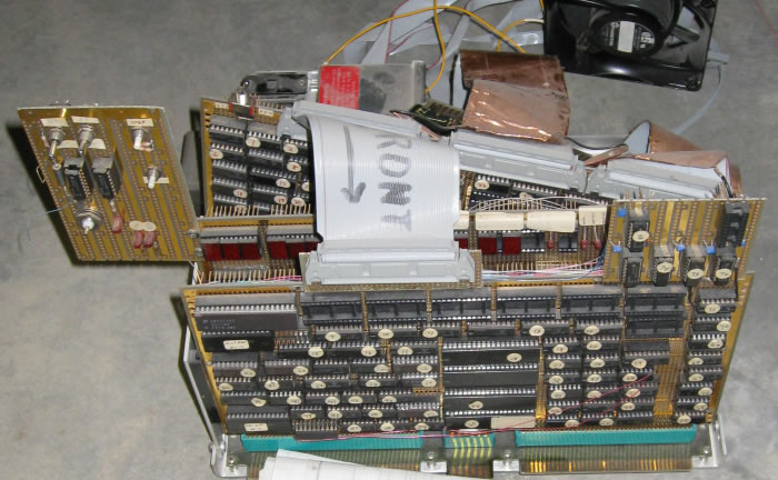
9845 Option 200 Bit-slice Processor Assembly
The bit-slice processor consisted of one lean connector board, and three boards packed with the 2900 chips, the PROMs and a large number of discrete logic chips. The whole construction has a high board and chip density, and it has some weight. However, though it gets really tight, it still fits into the LPU slot. And despite the complexity of the whole package, the bit-slice processors today still work fine (at least the two I got). Unfortunatly, the PROMs are not socketed, so it will be hard to create backup copies.
Bit-slice Processor Prototype (Wire Wrapped)
Photo Courtesy of Marl Godfrey
The bit-slice processor requires a couple of new ROM revisions at the LPU side. The old LPU ROMs with the part numbers 1818-0823 to 1818-0830 have to be replaced by the ROMs with the part numbers 1818-1502 to 1818-1509. Apparently, also the PSU should be upgraded to the A81 assembly in order to meet the power requirements of the 9845 option 200 models.
Processor Pinout
The processor pinout changed slightly between the different revisions. The original design without Address Extension Chip (as used in the 9825 and the 9845A) had 82 contacts (with a 14 x 27 layout). The later 9845B/C version with the integrated AEC (which was also used in the 9835 systems) had a completely revised scheme with 107 connections on a 20 x 38 contact raster (some power supply and ground connections used two contacs). Some signals which didn't proove important had been abandoned, others had been added (especially the memory address extension lines).
Back View of the 9845A Hybrid Processor with the VLSI Chips below the sealed Substrate Lid
Back View of the 9845B/C Hybrid Processor
Please note that both the 9825 CPU and the 9845A LPU/PPU have the same size and contact layout but differ slightly in signal assignment. The hole in the lid was used to produce a vaccuum during the production process and was sealed afterwards.
The numbering on both the substrate and the PCB refers to the connections (=signals), not to the contact raster. Here is an overview with some reference to the signal names Tony Duell used in his 9845B schematics (sometimes I can just guess because the documentation lacks any datails, so please use those information with care).
| Mnemonic | Pinout | I/O | Description | |||
| HP | Duell | 9825 | 9845A | 9845B | ||
| IRH/ | IRH/ | 1 | 1 | I | Interrupt Request line (high priority): an external device requests an interrupt by forcing this line low. IRH has a higher priority than interrupt request low (IRL), and can preempt the lower priority interrupt even while it is in process. POP can preempt IRH. | |
| IRL/ | IRL/ | 2 | 2 | I | Interrupt Request line (low priority): an external device requests an interrupt by pulling this line low. IRL is the lowest priority interrupt, and has no preempt abilities, therefore, must wait on its turn. IRH and POP can preempt IRL. | |
| EXBG, EBG | 3 | O | Extended or External Bus Grant: when high, indicates the requesting device that it may use the ID Address Bus (IDA). | |||
| KLSel | 3 | ? | KDP/processor select (?) | |||
| DMAR/ | DMAR/ | 4 | 4 | I | DMA Request line: a peripheral device forces this line low when it wants to access memory. | |
| +12V IOC | 5 | 5 | +12V Power Supply (IOC) | |||
| IC2/ | IC2/ | 6 | 6 | 1 | O | Interface Control 2 (n/c on LPU): one of two lines which can provide up to four states used to control peripheral devices. How these lines are controlled is determined by software (usually to select one of four peripheral device registers). |
| IC1/ | IC1/ | 7 | 7 | 2 | O | Interface Control 1 (n/c on LPU): one of two lines which can provide up to four states used to control peripheral devices. How these lines are controlled is determined by software (usually to select one of four peripheral device registers). |
| BE/ | IBE/ | 8 | 8 | 3 | O | I/O Buffer Enable (n/c for 9825 and 9845B LPU) |
| DOUT/ | DOUT/ | 9 | 9 | 4 | O | I/O Direction Control (n/c on LPU): when low, indicates to the addressed peripheral device that the processor will write data to it. IOSB must also be low. |
| IOSB/ | IOSB/ | 10 | 10 | 5 | O | I/O Strobe (n/c on LPU): when low, indicates that the data on the input/output bus (IOD) is valid. |
| POP/ | POP/ | 11 | 11 | I | Power On Pre-set (input from PSU): when low, initializes and prevents the microprocessor from running. When POP is released, the microprocessor begins operation at address 20 hex. POP is synchronized with CLK2 before being input to the microprocessor. POP can preempt IRL and IRH. | |
| ERA/ | TestA | 6 | I | Extended Register Access (n/c on PPU): when forced low by an external device, the internal registers have increased addressing range on the ID Address bus (IDA). | ||
| PDR/ | 7 | ? | Processor is Driving (n/c): when low, the microprocessor is driving the instruction/data/address bus (IDA). | |||
| +12V EMC | +12V | 12 | 12 | 8 | +12V Power Supply (EMC) | |
| DC/ | 9 | ? | Decimal Carry (n/c) | |||
| +7V | +7.5V | 10 | +7V Power Supply | |||
| BSC0/ | UA16 | 11 | O | Memory Address Extension line 0 | ||
| BSC1/ | UA17 | 12 | O | Memory Address Extension line 1 | ||
| BSC2/ | UA18 | 13 | O | Memory Address Extension line 2 | ||
| BSC3/ | UA19 | 14 | O | Memory Address Extension line 3 | ||
| BSC4/ | UA20 | 15 | O | Memory Address Extension line 4 | ||
| BSC5/ | UA21 | 16 | O | Memory Address Extension line 5 | ||
| 17 | O | Memory Address Extension line 6 (n/c) | ||||
| 18 | O | Memory Address Extension line 7 (n/c) | ||||
| 19 | O | Memory Address Extension line 8 (n/c) | ||||
| 20 | O | Memory Address Extension line 9 (n/c) | ||||
| 21 | O | Memory Address Extension line 10 (n/c) | ||||
| 22 | O | Memory Address Extension line 11 (n/c) | ||||
| 23 | O | Memory Address Extension line 12 (n/c) | ||||
| 24 | O | Memory Address Extension line 13 (n/c) | ||||
| 25 | O | Memory Address Extension line 14 (n/c) | ||||
| 26 | O | Memory Address Extension line 15 (n/c) | ||||
| +12V AEC | +12V | 27 | +12V Power Supply (AEC) | |||
| DC/ | 13 | 13 | I | Decimal Carry (n/c for 9825), for the 9845A PPU connected to CRT vertical retrace | ||
| PDR/ | 14 | 14 | O | Processor is Driving (n/c for 9825): when low, the microprocessor is driving the instruction/data/address bus (IDA). | ||
| FLG/ | FLG/ | 15 | 15 | 28 | I | Flag (PPU only, connected to +7V on 9845A LPU or +12V on 9845B LPU): can be tested by software. A hardware line used as 'flag' by any peripheral device which is connected to the microprocessor. There are wire ORed 'flags'. |
| STS/ | STS/ | 16 | 16 | 29 | I | Status (PPU only, connected to +7V on 9845A LPU or derived from HLT/ signal on 9845B LPU): can be tested by software. Used as a 'flag' by any peripheral device connected to the microprocessor. the peripheral devices are wire ORed to this line. |
| HLT/ | VAck/ | 17 | 17 | 30 | I | Halt (n/c for 9825, for the 9845B/C PPU connected to CRT vertical retrace, for the 9845B/C LPU grounded): can be tested by software. Used as a 'flag' to the microprocessor by the system bus controller for interrupts (9845A) or for testing vertical retrace (9845B/C PPU). |
| RELA/ | +12V | 31 | Relative Addressing (connected to +12V) | |||
| +7V BPC,EMC | +7.5V | 18 | 18 | 32 | +7V Power Supply (BPC, EMC) | |
| +12V BPC | +12V | 33 | +12V Power Supply (BPC) | |||
| CLEAN GND | Gnd | 34 | Ground | |||
| CLEAN GND | Gnd? | 19 | 19 | ? | Ground | |
| 02 | 02out | 20 | 20 | 35 | O | Clock 2 out: one of two complementary, non-overlapping clocks. Required by the microprocessor chip. |
| CLK | Clk | 36 | I | Clock in | ||
| 01 | 01out | 21 | 21 | 37 | O | Clock 1 out: one of two complementary, non-overlapping clocks. Required by the microprocessor chip. |
| CLEAN GND | Clean | 22 | 22 | 38 | I | Ground |
| +12V BPC | +12V | 23 | 23 | +12V Power Supply (BPC) | ||
| CLK IN | Clk | 24 | 24 | I | Clock in (n/c for 9825) | |
| UMC/ | TestRet | 25 | 25 | 39 | I | Unsynchronized Memory Complete: when low, allows the microprocessor to complete its memory cycle. If the memory needs to make the microprocessor wait, due to long access times, it pulls UMC high. When UMC is high, the microprocessor must wait. |
| DSTM/ | 26 | 26 | O | Delayed Start Memory (n/c for 9825) | ||
| INT/ | INT/ | 27 | 27 | I/O | Interrupt control (IOC:output, BPC/EMC:input): the microprocessor pulls this line low in response to IRH and IRL to allow polling the input/output bus to determine which peripheral requested the interrupt. | |
| STMR/ | 40 | ? | Start Memory ROM (n/c) | |||
| ERA/ | 28 | 28 | I | Extended Register Access: when forced low by an external device, the internal registers have increased addressing range on the ID Address bus (IDA). | ||
| PON | 41 | I | Power On Signal (derived from INIT/ signal) | |||
| SNYC/ | Inst/ | 29 | 29 | I/O | Instruction fetch synchronization: when high, indicates the microprocessor is fetching an opcode. | |
| STM/ | STM/, ALE/ | 30 | 30 | 42 | I/O | Start Memory: used to initiate a memory cycle. When low, indicates that the information on the address bus is valid. |
| WRT/ | WrEn/ | 31 | 31 | 43 | I/O | Read/Write: when high, indicates the microprocessor will read from devices external to it. When low, the processor will write to devices such as memory. |
| BG | ArbEn/ | 32 | 32 | O | Bus Grant: when high, acknowledges Low Bus request has been received. However the requesting device mus waot until High External Bus Grant (EBG) is true before using the IDA Bus. | |
| SMC/ | ALEEn/, EnHi/ | 33 | 33 | 44 | I/O | Synchronized Memory Complete |
| RAL | InitOut/ | 34 | 34 | 45 | O | Register Access Line: when an address on the ID Address Bus (IDA) is within the range reserved for register designation, RAL goes high to prevent external memeory from responding to any memory cycle havinf the same address. |
| -5V BPC | -5V | 35 | 35 | 46 | -5V Power Supply (BPC) | |
| -5V AEC | -5V | 47 | -5V Power Supply (AEC) | |||
| -5V EMC | -5V | 36 | 36 | 48 | -5V Power Supply (EMC) | |
| +5V | +5V | 37 | 37 | 49 | +5V Power Supply | |
| DIRTY GND | Gnd | 38 | 38 | 50 | I | Ground |
| +7V BIB | +7.5V | 51 | +7V Power Supply | |||
| IDA8/ | AD8 | 39 | 39 | I/O | Instruction Data Address bus line 8 | |
| IDA9/ | AD9 | 40 | 40 | I/O | Instruction Data Addressbus line 9 | |
| IDA10/ | AD10 | 41 | 41 | I/O | Instruction Data Address bus line 10 | |
| IDA11/ | AD11 | 42 | 42 | I/O | Instruction Data Address bus line 11 | |
| IDA12/ | AD12 | 43 | 43 | I/O | Instruction Data Address bus line 12 | |
| IDA13/ | AD13 | 44 | 44 | I/O | Instruction Data Address bus line 13 | |
| IDA14/ | AD14 | 45 | 45 | I/O | Instruction Data Address bus line 14 | |
| IDA15/ | AD15 | 46 | 46 | 52 | I/O | Instruction Data Address bus line 15 |
| IDA14/ | AD14 | 53 | I/O | Instruction Data Address bus line 14 | ||
| IDA13/ | AD13 | 54 | I/O | Instruction Data Address bus line 13 | ||
| IDA12/ | AD12 | 55 | I/O | Instruction Data Address bus line 12 | ||
| IDA11/ | AD11 | 56 | I/O | Instruction Data Address bus line 11 | ||
| IDA10/ | AD10 | 57 | I/O | Instruction Data Address bus line 10 | ||
| IDA9/ | AD9 | 58 | I/O | Instruction Data Address bus line 9 | ||
| IDA8/ | AD8 | 59 | I/O | Instruction Data Address bus line 8 | ||
| +7V BIB | +7.5V | 60 | I/O | +7V Power Supply (BIBs) | ||
| IDA7/ | AD7 | 47 | 47 | 61 | I/O | Instruction Data Address bus line 7 |
| IDA6/ | AD6 | 48 | 48 | 62 | I/O | Instruction Data Address bus line 6 |
| IDA5/ | AD5 | 49 | 49 | 63 | I/O | Instruction Data Address bus line 5 |
| IDA4/ | AD4 | 50 | 50 | 64 | I/O | Instruction Data Address bus line 4 |
| IDA3/ | AD3 | 51 | 51 | 65 | I/O | Instruction Data Address bus line 3 |
| IDA2/ | AD2 | 52 | 52 | 66 | I/O | Instruction Data Address bus line 2 |
| IDA1/ | AD1 | 53 | 53 | 67 | I/O | Instruction Data Address bus line 1 |
| IDA0/ | AD0 | 54 | 54 | 68 | I/O | Instruction Data Address bus line 0 |
| IBE/, PBE/ | Gnd | 69 | I | Buffer Enable: IBE/ on LPU, PBE/ on PPU (grounded): enables the internal microprocessor buffers for the instruction/data/address bus (IDA). | ||
| IBO/, PBO/ | Dir | 70 | I | Buffer Direction Control: IBO/ on LPU, PBO/ on PPU (grounded on LPU): controls the direction of the microprocessor's internal, bidirectional, ID address (IDA) buffers. When low, information is transmitted from the microprocessor. | ||
| +7V BIB | +7.5V | 55 | 55 | 71 | +7V Power Supply (BIBs) | |
| IOD7/ | IOD7 | 56 | 56 | I/O | I/O Data bus line 7 (n/c on LPU) | |
| IOD6/ | IOD6 | 57 | 57 | I/O | I/O Data bus line 6 (n/c on LPU) | |
| IOD5/ | IOD5 | 58 | 58 | I/O | I/O Data bus line 5 (n/c on LPU) | |
| IOD4/ | IOD4 | 59 | 59 | I/O | I/O Data bus line 4 (n/c on LPU) | |
| IOD3/ | IOD3 | 60 | 60 | I/O | I/O Data bus line 3 (n/c on LPU) | |
| IOD2/ | IOD2 | 61 | 61 | I/O | I/O Data bus line 2 (n/c on LPU) | |
| IOD1/ | IOD1 | 62 | 62 | I/O | I/O Data bus line 1 (n/c on LPU) | |
| IOD0/ | IOD0 | 63 | 63 | I/O | I/O Data bus line 0 (n/c on LPU) | |
| PBE/ | Gnd | 64 | 64 | I | Processor buffer enable (IDA-bus) (grounded for 9825): enables the internal microprocessor buffers for the instruction/data/address bus (IDA). | |
| PBO/ | Out/ | 65 | 65 | I | Processor buffer direction control (IDA-bus): controls the direction of the microprocessor's internal, bidirectional, ID address (IDA) buffers. When low, information is transmitted from the microprocessor. | |
| IOD15/ | IOD15 | 66 | 66 | I/O | I/O Data bus line 15 (n/c on LPU) | |
| IOD14/ | IOD14 | 67 | 67 | I/O | I/O Data bus line 14 (n/c on LPU) | |
| IOD13/ | IOD13 | 68 | 68 | I/O | I/O Data bus line 13 (n/c on LPU) | |
| IOD12/ | IOD12 | 69 | 69 | I/O | I/O Data bus line 12 (n/c on LPU) | |
| IOD11/ | IOD11 | 70 | 70 | I/O | I/O Data bus line 11 (n/c on LPU) | |
| IOD10/ | IOD10 | 71 | 71 | I/O | I/O Data bus line 10 (n/c on LPU) | |
| IOD9/ | IOD9 | 72 | 72 | I/O | I/O Data bus line 9 (n/c on LPU) | |
| IOD8/ | IOD8 | 73 | 73 | I/O | I/O Data bus line 8 (n/c on LPU) | |
| IOD0/ | IOD0 | 72 | I/O | I/O Data bus line 0 (n/c on LPU) | ||
| IOD1/ | IOD1 | 73 | I/O | I/O Data bus line 1 (n/c on LPU) | ||
| IOD2/ | IOD2 | 74 | I/O | I/O Data bus line 2 (n/c on LPU) | ||
| IOD3/ | IOD3 | 75 | I/O | I/O Data bus line 3 (n/c on LPU) | ||
| IOD4/ | IOD4 | 76 | I/O | I/O Data bus line 4 (n/c on LPU) | ||
| IOD5/ | IOD5 | 77 | I/O | I/O Data bus line 5 (n/c on LPU) | ||
| IOD6/ | IOD6 | 78 | I/O | I/O Data bus line 6 (n/c on LPU) | ||
| IOD7/ | IOD7 | 79 | I/O | I/O Data bus line 7 (n/c on LPU) | ||
| +7V BIB | +7.5V | 80 | +7V Power Supply | |||
| IOD8/ | IOD8 | 81 | I/O | I/O Data bus line 8 (n/c on LPU) | ||
| IOD9/ | IOD9 | 82 | I/O | I/O Data bus line 9 (n/c on LPU) | ||
| IOD10/ | IOD10 | 83 | I/O | I/O Data bus line 10 (n/c on LPU) | ||
| IOD11/ | IOD11 | 84 | I/O | I/O Data bus line 11 (n/c on LPU) | ||
| IOD12/ | IOD12 | 85 | I/O | I/O Data bus line 12 (n/c on LPU) | ||
| IOD13/ | IOD13 | 86 | I/O | I/O Data bus line 13 (n/c on LPU) | ||
| IOD14/ | IOD14 | 87 | I/O | I/O Data bus line 14 (n/c on LPU) | ||
| IOD15/ | IOD15 | 88 | I/O | I/O Data bus line 15 (n/c on LPU) | ||
| IO Dout/ | 74 | ? | ? | |||
| DIRTY GND | 74 | ? | Ground | |||
| PBE/, IBE/ | IOT | 89 | I | Buffer Enable: PBE/ on LPU, IBE/ on PPU (grounded on LPU): enables the internal microprocessor buffers for the instruction/data/address bus (IDA). | ||
| PBO/, IBO/ | IODEn | 90 | I/O | Buffer Direction Control: PBO/ on LPU, IBO/ on PPU (connected to DOUT/ on PPU): controls the direction of the microprocessor's internal, bidirectional, ID address (IDA) buffers. When low, information is transmitted from the microprocessor. | ||
| DIRTY GND | Gnd | 91 | Ground | |||
| -5V IOC | -5V | 75 | 75 | 92 | -5V Power Supply (IOC) | |
| BYTE/ | WordWr | 76 | 76 | O | Byte interpretation: when low, indicates that a memory cycle is to invlove an eight bit byte, rather than the full sixteen bits of the word. | |
| PAB3/ | PA3 | 77 | 77 | 93 | O | Peripheral Address Bus line 3 (n/c on LPU) |
| PAB2/ | PA2 | 78 | 78 | 94 | O | Peripheral Address Bus line 2 (n/c on LPU) |
| PAB1/ | PA1 | 79 | 79 | 95 | O | Peripheral Address Bus line 1 (n/c on LPU) |
| PAB0/ | PA0 | 80 | 80 | 96 | O | Peripheral Address Bus line 0 (n/c on LPU) |
| BYTE/ | WordWr | 97 | O | Byte interpretation: when low, indicates that a memory cycle is to invlove an eight bit byte, rather than the full sixteen bits of the word. | ||
| BR/ | 81 | 81 | I | Bus Request: provides the way for an external device to request uninterrupted use of the ID Address Bus (IDA). | ||
| BL/ | U/L | 82 | 82 | 98 | O | Byte Left: Determines which half of a word will be affected (BL/ low: MSB, BL/ high: LSB) |
| INT/ | INT/ | 99 | I/O | Interrupt control (IOC:output, BPC/EMC:input) (n/c on LPU): the microprocessor pulls this line low in response to IRH and IRL to allow polling the input/output bus to determine which peripheral requested the interrupt. | ||
| BG | TestC | 100 | O | Bus Grant: when high, acknowledges Low Bus request has been received. However the requesting device mus waot until High External Bus Grant (EBG) is true before using the IDA Bus. | ||
| IRH/ | IRH/ | 101 | I | Interrupt Request line (high priority) (connected to +12V on LPU): an external device requests an interrupt by forcing this line low. IRH has a higher priority than interrupt request low (IRL), and can preempt the lower priority interrupt even while it is in process. POP can preempt IRH. | ||
| IRL/ | IRL/ | 102 | I | Interrupt Request line (low priority) (connected to +12V on LPU): an external device requests an interrupt by pulling this line low. IRL is the lowest priority interrupt, and has no preempt abilities, therefore, must wait on its turn. IRH and POP can preempt IRL. | ||
| EXBG, EBG | VAEn | 103 | O | Extended or External Bus Grant: when high, indicates the requesting device that it may use the ID Address Bus (IDA). | ||
| DMAR/ | DMAR/ | 104 | I | DMA Request (connected to +12V on LPU): a peripheral device forces this line low when it wants to access memory. | ||
| BR/ | VRq/ | 105 | I | Bus Request: provides the way for an external device to request uninterrupted use of the ID Address Bus (IDA). | ||
| SYNC/ | TestB | 106 | ? | Instruction fetch synchronization | ||
| +12V IOC | +12V | 107 | +12V Power Supply (IOC) | |||
The following signals exist but could not be assigned (probably CTE, GNI/ and DVAL/ are used by the test connector, e.g. as TestA, TestB and TestC):
| CTE | Counter Test Enable |
| GNI/ | Get Next Instruction |
| DVAL/ | Data Valid |
| ODD | Output Driver Disable (internal signal, no pin connected) |
Processor Speed and Timing
All 9845 processors were internally clocked with 5.7 MHz, derived from an external 11.4 MHz clock signal. One processor clock cycle was 175 nanoseconds. The fastest instruction, a program pointer change (JMP), needed 8 clock cycles, whereas the longest instruction, a BCD floating point multiply, needed 65 clocks. So the processor could perform at ~0.7 MIPS, which was approximately the speed of an Intel 8088/8086 microprocessor. The floating point performance was about 0.15 MFLOPS (floating point addition), which was significantly faster than an 8087 maths coprocessor.
A speciality of the 9845 processors were fast block operations, which could be used to copy or zero a block of up to 16 words with one single instruction. The XFR instruction for copying the content of a memory block to another address could consume up to 213 clocks for a 16-words block, but was much faster and more convenient than an instruction loop which did the same. A 16-word memory clear needed only 112 clocks, so that a complete 32 KWord (64 KBytes) memory block could be cleared in less than 50 ms, and the max. memory installation of 1.5 MBytes in just 1.2 seconds.
The bit-slice implementation of the LPU probably didn't deviate too much from this timing, since the acceleration factor was related to the microcode implementation of several BASIC routines and didn't speed up machine code processing. Nevertheless, here is a comparison of the resulting BASIC performance (all measures are in ms):
BASIC Routine |
Standard Hybrid LPU |
Bit-slice LPU |
Acceleration Factor |
Addition |
0.27 | 0.04 | 6.75 |
Subtraction |
0.33 | 0.06 | 5.50 |
Multiplication |
0.89 | 0.14 | 6.35 |
Division |
2.90 | 0.56 | 5.18 |
Raise to Power |
17.00 | 3.21 | 5.30 |
Square Root |
2.90 | 0.43 | 6.75 |
Tangent |
14.00 | 2.41 | 5.81 |
Sine |
21.00 | 3.68 | 5.71 |
Cosine |
21.00 | 3.68 | 5.71 |
Arctangent |
18.00 | 2.31 | 7.80 |
Arcsine |
26.00 | 3.88 | 6.70 |
Arccosine |
26.00 | 4.00 | 6.50 |
Natural Log |
7.50 | 1.39 | 5.40 |
Log Base 10 |
9.70 | 1.49 | 6.51 |
ex |
6.10 | 1.00 | 6.00 |
Integer |
0.46 | 0.24 | 1.92 |
Absolute Value |
0.13 | 0.03 | 4.33 |
Fraction |
0.35 | 0.09 | 3.89 |
Random Number |
1.80 | 0.33 | 5.46 |
Other Microcontrollers
The 9845 architecture is based on the concept of "distributed intelligence", so beside the two CPU's there is a large number of VLSI chips including a couple of microcontrollers disburdening the CPU's from several tasks. Most VLSI chips are custom HP designs, however some of the interface modules are using standard microcontrollers from other vendors, like the Datacomm Interface which uses an Intel 8048 microcontroller.
The BPC Processor
The BPC processor was a strip-down version of the 16-bit 9845 hybrid with only a BPC chip. It was used as controller for the HP 9871A daisy-wheel impact printer (introduced in 1975) and later in the 9872 series plotters (introduced 1977), as well as for the 9874A digitizer and the 9875A dual tape cartridge drive (both introduced in 1978). Primary usage was as logic controller when 16-bit word processing was required, mostly in combination with other interface or device controllers.
In case 8-bit wide processing was applicable, another processor, the "nanoprocessor" was the choice (see next paragraph).
 BPC Processor Pinout |
BPC Ceramic Package |
The Nanoprocessor
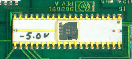 For most 8-bit controller tasks at the time of the 9845, HP used its own development, an 8-bit microprocessor called "nanoprocessor" (P/N 1820-1692).
This processor was also used as controller for the 9845 series thermal printer. The 9845 thermal printer is a complex system consisting of the printer mechanics, a printer motor control circuit and a printer logic assembly. The printer subsystem is connected to the 9845 PPU via the IOD bus. Actually, the printer subsystem is an independent computer with the IOD bus as host interface. The nanoprocessor was clocked with 8 MHz. It featured a complete logic & I/O controller system, including 16 internal 8-bit registers, an 11-bit program address space, an 8-bit data bus, 3 interrupt lines, 4 device select lines, and 7 I/O lines.
In addition to the nanoprocessor, the printer control assembly holds 2 kBytes of printer control firmware, a 2 kByte character ROM and 256 Bytes of read/write memory.
Note the hand-written back bias voltage value (-5.0 V on the sample above). There was a possible range between -2.0 and -5.0 V in .5 V steps. Obviously, HP's manufacturing process of the nanoprocessor produced chips with different tolerances, so each chip had to be tested individually. The required back bias voltage then was established by selecting the appropriate resistor on the PCB. This should be taken into account when replacing a nanoprocessor.
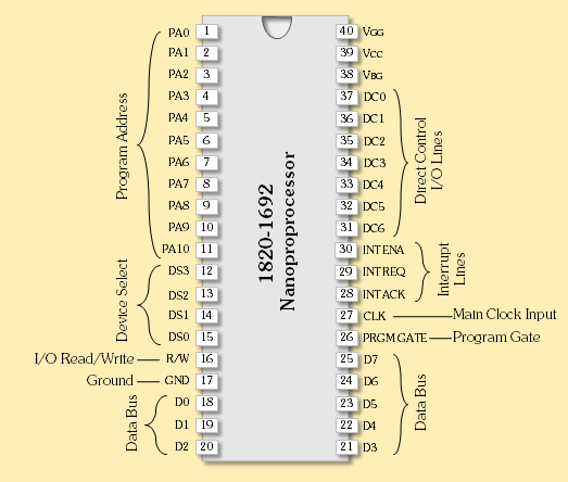
9845 Internal Thermal Printer Microcontroller (P/N 1820-1692) Pinout
The nanoprocessor was also used in the 98034 HP-IB interface and in the 98035 Real Time Clock interface.
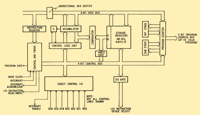
9845 Internal Thermal Printer Microcontroller Block Diagram
You can download the orginal Nanoprocessor User's Guide here (draft version courtesy Larry Bower and Paul Berger).The Tape Drive Controller (TACO)
The tape drive controller (TACO) chip was a new NMOSIII-development integrating 48 TTL logic chips and 80 discrete components into one single controller chip. The TACO chip was used in the 9845 series, in the 64940A tape controller (as part of the 64000 logic development system) and in the 9875A dual tape cartridge unit.
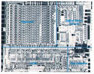
TACO Chip Layout and TACO on PCB with Heatsink
Compared to the original 9825 tape controller logic, the TACO chip did not only replace the low level TTL logic, but provided also high-level tape control functions for the PPU. The controller was clocked with 4 MHz and interfaced to the PPU via the IOD bus. It was completely self-contained and didn't need any external RAM or ROM components.
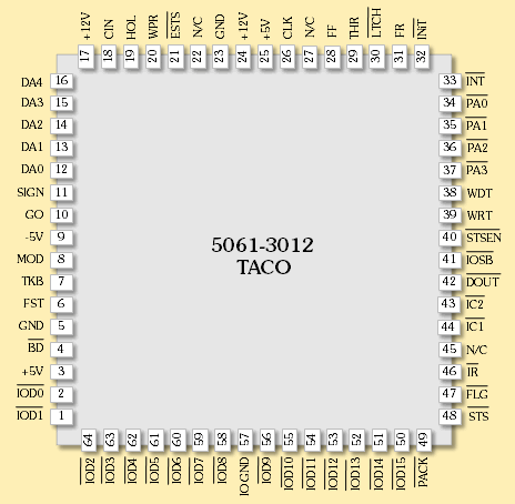
5061-3012 Tape Controller Chip Pinout
The (for now) probably most comprehensive official description of the TACO chip and its command set can be found within the 64940-90905 Tape Control And Drive Service Manual. The TACO chip uses the following registers:
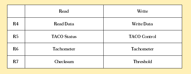
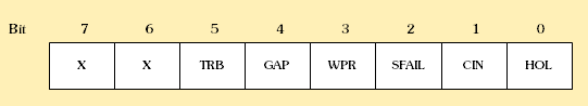
R5 works as status and control register. The individual bits of the TACO status register are assigned as follows:
with:
| Bit 0 | HOL - hole detect (1 = hole, 0 = not hole) |
| Bit 1 | CIN - cartridge detect (1 = cartridge out, 0 = cartridge in) |
| Bit 2 | SFAIL - servo fail detect (1 = servo fail, 0 = servo OK) |
| Bit 3 | WPR - write protect detect (1 = write protected, 0 = not write protected) |
| Bit 4 | GAP - gap detect (1 = in gap, 0 = not in gap) |
| Bit 5 | TRB - current track (1 = track B, 0 = track A) |
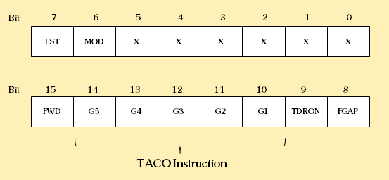
A write to the TACO control register starts execution of the TACO command selected by an instruction code. The individual bits of the TACO control register are assigned as follows:
with:
| Bit 0 - 5 | not used |
| Bit 6 | MOD - depends on instruction, e.g. threshold (1 = high volt threshold, 0 = low volt threshold) |
| Bit 7 | FST - tape speed (1 = fast/90 ips, 0 = slow/22 ips) |
| Bit 8 | FGAP - minimum gap size detected (1 = 1.5", 0 = 0.066") |
| Bit 9 | TDRON - automatic stop on command completion (1 = stop, 0 = don't stop) |
| Bit 10 - 14 | G1 to G5 - Instruction code |
| Bit 15 | FWD - tape direction (1 = forward, 0 = reverse) |
Not all of the 32 instructions have been discovered yet, here are the ones which are used by the 9845 firmware and where we have some idea of (thanks to F.Ulivi's re-engineering efforts):
| Instruction | Description |
0 |
Scan for data, then for gap |
2 |
Write EVD (end of valid data) gap |
3 |
Initialize tape with data |
4 |
Stop tape |
6 |
Set current track |
10 |
Start continuous tape movement |
12 |
Scan for gap, then move for a given distance |
14 |
Clear errors and unlatch status bit |
16 |
Same as command 0 |
22 |
Write a gap of given length |
24 |
Scan for gaps |
25 |
Write data |
26 |
Move for a given distance, then scan for data |
27 |
NOP (?) |
28 |
Move for a given distance, then scan for a gap |
29 |
Start reading data |
30 |
Move for a given distance |
31 |
End reading data |
F.Ulivi has written a comprehensive description of his findings on the TACO chip, where the use of the above commands is described in detail.
R6 is a read/write register counting upward either tachometer pulses or gaps, depending on the current command. A 16-bit roll-over normally terminates the ongoing command. Counting is "freezed" when writing to this register. The register is reset by the TACO command which uses this register.
R7, when read, returns the checksum of all words being exchanged with the tape since the last read to this register. The checksum is built by simply adding the next data word to the current content of this register, and storing the result modulo 216 back to this register. Writing to this register controls pre-compensation and one/zero threshold. The exact use is yet unknown, usually a 0x661d is written to this register on writes to tape, and 0x0625 on tape reads (0x061d for SIF utilities).
The TACO chip is enabled by select code 12 at PA0 to PA3, which is internally mapped by the HP9845 to either select code 15 (primary tape drive) or select code 14 (secondary tape drive) within the HP9845.
Display Controllers
The display controllers of the 98750A standard graphics display was completely built with discrete TTL logic, whereas the 98770A color display used a special vector acceleration hardware based on a fast, general purpose AMD bit-slice processor setup.
5061-4203 Graphics Controller (back view, heat sink)
The 5061-4203 graphics controller was part of the 98780A enhanced monochrome graphics display. This controller was responsible for (at the time) light speed graphics performance with hardware accelerated vector and circle generation. The 5061-4203 graphics controller also implemented the so-called rubber band feature in hardware, a graphics object which could be drawn and moved along the screen without destroying the pixel data.
Interface Controllers
To be continued...
More Information
See Steve Leibson's great hp9825.com site for more information on the history and internals of HP's hybrid processors. Also have a look at Accutron's arcticle discussing the hybrid processors at the Vintage Technology Association.
The different function groups inside the hybrids are deeply described in the 9825 and 9845 patent documents, please have a look into the patents section.